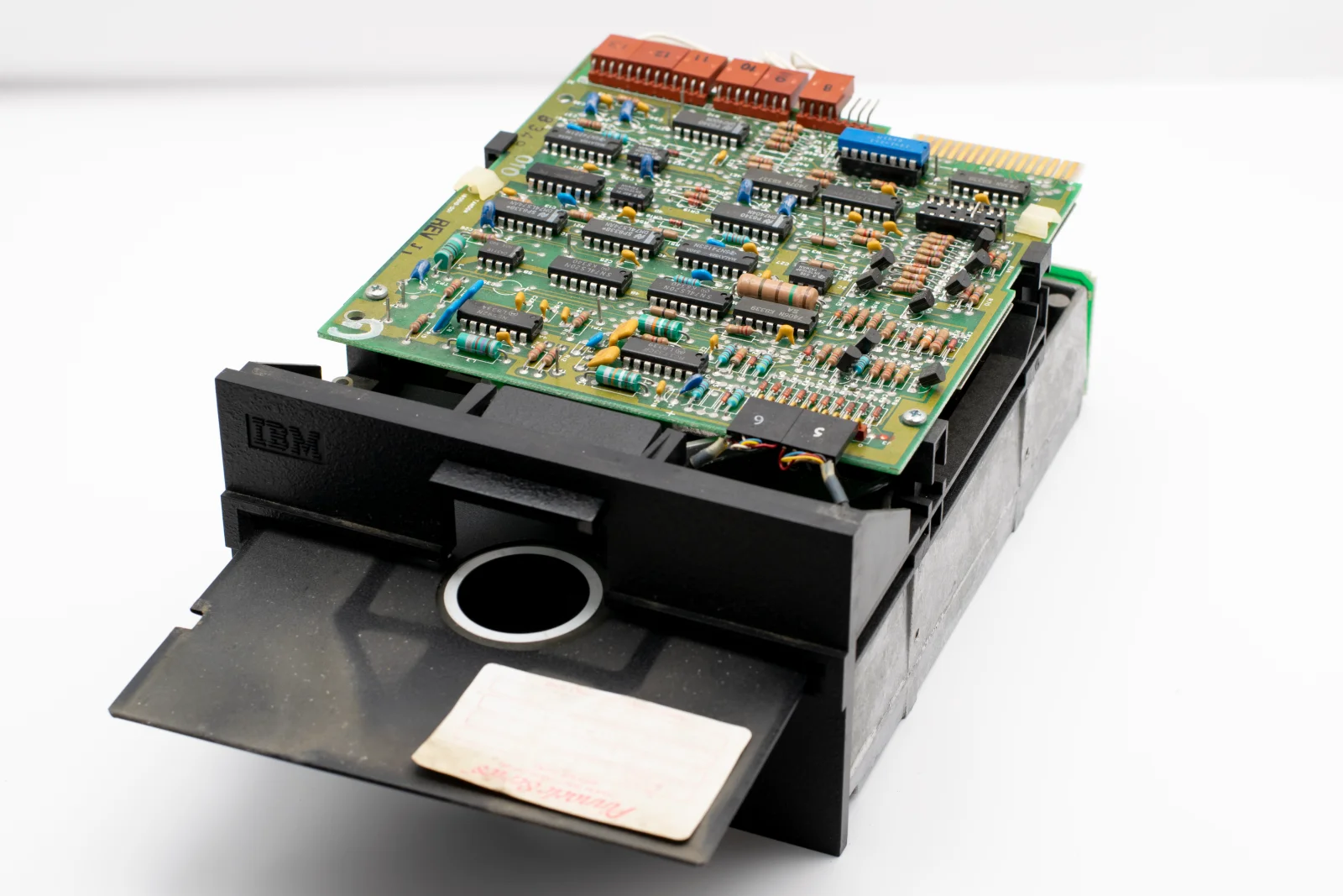
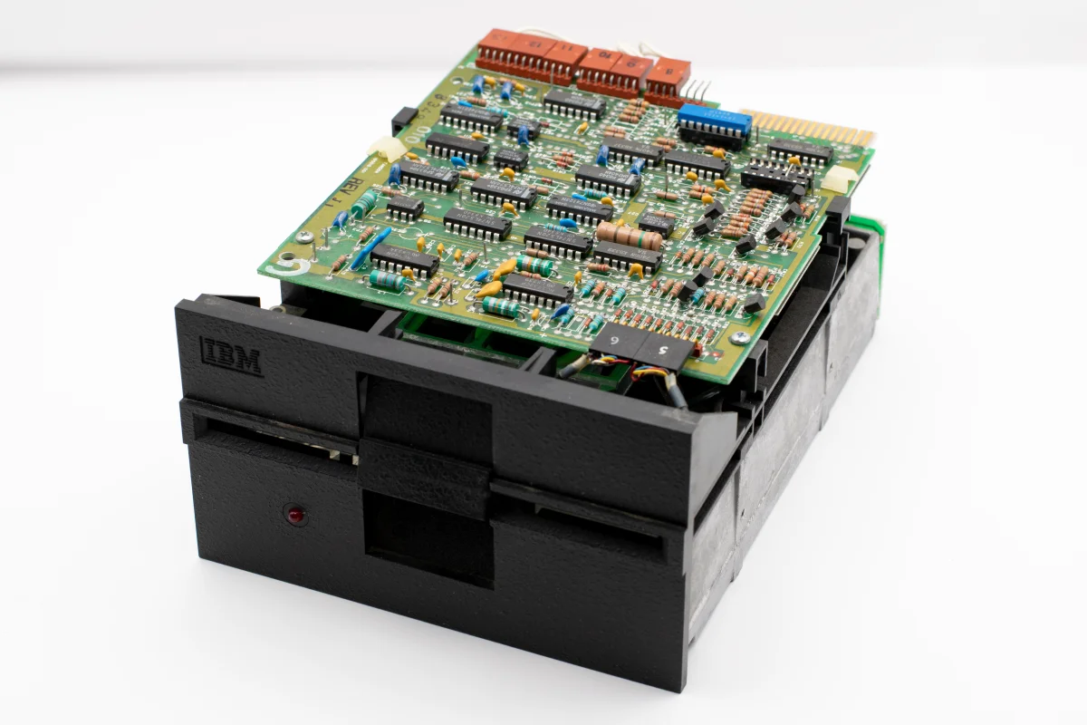
The world of microprocessors has witnessed a groundbreaking achievement as IBM announces the development of the first sub-1 nanometer chip technology. This innovation marks a significant leap forward, promising to redefine the capabilities of modern computing. With this advancement, IBM not only pushes the boundaries of semiconductor technology but also sets a new standard for energy efficiency and processing power, potentially transforming industries reliant on computational prowess.
Chapter 01
The Breakthrough
Exploring the implications of IBM's sub-1 nanometer chip technology.
Understanding the Technology
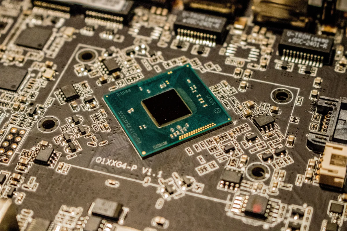
IBM’s sub-1 nanometer technology is a marvel of engineering, achieving unprecedented miniaturization. Nanotechnology allows for the construction of chips with features smaller than a single nanometer, vastly increasing the number of transistors that can be packed into a microprocessor. This breakthrough enhances performance, reduces power consumption, and opens new avenues for innovation.
- Miniaturization: Smaller transistors increase chip density.
- Efficiency: Enhanced energy efficiency with lower power requirements.
- Performance: Significant improvements in speed and processing power.
- Scalability: Potential for further advancements in microelectronics.
- Applications: Expands capabilities in AI, cloud computing, and IoT.
- Sustainability: Reduced environmental impact through efficient energy use.
The Science Behind It
The development of sub-1 nanometer chips involves intricate material science and advanced lithography techniques. By utilizing extreme ultraviolet (EUV) lithography, IBM engineers can etch incredibly fine patterns onto silicon wafers, enabling the creation of these minuscule transistors. This precision is critical for achieving the desired performance gains.
Historical Context
The journey to sub-1 nanometer technology is rooted in decades of research and development. Historically, the semiconductor industry has followed Moore’s Law, which predicts the doubling of transistors on a chip approximately every two years. IBM’s innovation represents a pivotal moment, transcending traditional scaling limitations and establishing a new frontier for chip design.
The future of computing is defined by our ability to innovate at the atomic level.
Chapter 02
Applications and Implications
Exploring the potential uses and industry impact of sub-1 nanometer technology.
Narrative flow
Scroll through the argument
01
Enhancing AI
Sub-1 nanometer chips provide the computational power necessary for advanced AI applications, enabling faster processing of complex algorithms and data sets.
02
Revolutionizing Cloud Computing
These chips enhance the efficiency and scalability of cloud services, reducing latency and improving performance for end-users.
03
Driving IoT Innovation
With increased power and efficiency, sub-1 nanometer chips enable more sophisticated and energy-efficient IoT devices, expanding their potential applications.
AI and Machine Learning
Sub-1 nanometer chips are poised to transform artificial intelligence and machine learning. By delivering higher processing speeds and improved energy efficiency, these chips can handle the massive data sets and intensive computations required by AI systems, accelerating advancements in this field.
Cloud Computing Revolution
Cloud service providers stand to benefit immensely from this technology. Enhanced chip performance translates into more efficient data centers, capable of delivering faster and more reliable services to users. This could lead to a new era of cloud computing, characterized by unparalleled speed and scalability.
Common Misconceptions
Despite the excitement surrounding sub-1 nanometer technology, there are misconceptions about its capabilities. While these chips offer substantial benefits, they are not a panacea for all computing challenges. Practical implementation requires careful consideration of existing infrastructure and potential integration hurdles.
Visualizing the Future


The advent of sub-1 nanometer chip technology is a testament to human ingenuity and the relentless pursuit of progress. As this innovation takes hold, it promises to reshape industries and redefine what’s possible in technology. IBM has positioned itself at the forefront of this revolution, and the implications are profound. The world is on the brink of a new era in computing, driven by the power and potential of these cutting-edge chips.
Chapter 03
Future Directions
What lies ahead for sub-1 nanometer technology and the semiconductor industry?
Charting the Path Forward
The development of sub-1 nanometer chips is a critical milestone, but it also sets the stage for future challenges and opportunities. As the semiconductor industry evolves, companies must navigate technical hurdles, market demands, and the need for sustainable practices.
- Research and Development: Continued investment in R&D is essential for further advancements.
- Market Adaptation: Industries must adapt to leverage new capabilities effectively.
- Regulatory Considerations: Compliance with global standards and regulations is crucial.
- Sustainability: Emphasis on reducing environmental impact remains paramount.
- Collaboration: Partnerships across sectors can drive innovation and adoption.
- Customer Education: Educating stakeholders on benefits and limitations is key.
Real-World Implementation
Adopting sub-1 nanometer technology involves strategic planning and investment. Companies need to assess their current infrastructure, identify potential areas for improvement, and implement gradual transitions to integrate these advanced chips into their operations.
Best Practices and Recommendations
For organizations looking to capitalize on sub-1 nanometer advancements, embracing a forward-thinking mindset is crucial. This involves staying informed about technological trends, fostering a culture of innovation, and prioritizing sustainability in all aspects of business operations.
Chapter 04
The Long-Term Vision
Envisioning the impact of IBM's innovation on future technological landscapes.
A Vision for the Future
IBM’s sub-1 nanometer chip technology signals a new dawn for computing, one that promises unprecedented capabilities and efficiencies. As industries adapt to this new paradigm, the possibilities are endless. From AI to IoT, these innovations will redefine boundaries and drive progress in ways previously unimaginable.
Practical Implementation
To harness the full potential of sub-1 nanometer technology, organizations must prioritize adaptability and innovation. By investing in cutting-edge research and fostering collaboration, businesses can stay ahead of the curve and fully capitalize on these transformative advancements.
Trade-offs and Caveats
While the benefits are substantial, there are trade-offs to consider. The complexity and cost of developing and deploying sub-1 nanometer chips can be significant, requiring careful consideration and strategic planning to ensure successful implementation.
The journey toward sub-1 nanometer technology is just beginning, but its potential is already evident. IBM’s innovation represents a crucial step forward, offering a glimpse into a future where computing power knows no bounds. As we embrace these advancements, one thing is clear: the future will be defined by those who dare to innovate, pushing the limits of what’s possible.