Deep Dive
Precision in 2D Semiconductor Growth
Unlocking the potential of next-gen chips through controlled growth techniques.
The world of semiconductors is on the brink of a significant transformation. As industries push for smaller, more efficient chips, the role of 2D materials becomes increasingly critical. These atomically thin structures offer unique electrical properties, making them ideal candidates for next-generation semiconductors. But how can we control their growth to ensure consistent quality and performance? This question lies at the heart of a technological revolution that promises to redefine the future of chip manufacturing.
Chapter 01
The Potential of 2D Materials
Exploring the unique properties and advantages of 2D materials in semiconductor applications.
Understanding 2D Materials
2D materials, like graphene and transition metal dichalcogenides, are revolutionizing semiconductor technology. Their thinness allows for better electron mobility and faster processing speeds, qualities that are essential for modern devices. Yet, the challenge remains in controlling their growth with precision to harness these properties effectively.
- Enhanced Electron Mobility: 2D materials enable faster electron flow, reducing energy consumption.
- Scalability: Their atomic thickness allows for more compact chip designs, paving the way for miniaturization.
- Unique Electrical Properties: These materials offer tunable bandgaps, critical for specific semiconductor applications.

The world of semiconductors is on the brink of a significant transformation.
A semiconductor researcher
Challenges in Growth Control
While the benefits are clear, controlling the growth of 2D materials is fraught with challenges. Variability in thickness, defects, and alignment issues can hinder their performance. Advanced techniques are required to mitigate these problems and ensure uniformity across large areas.
Chapter 02
Techniques for Growth Control
Unveiling the latest methods for precise 2D material growth.
Innovative Growth Techniques
Recent advancements have introduced several innovative methods for controlling 2D semiconductor growth. These techniques aim to address the challenges of uniformity and defect reduction, ensuring that the potential of 2D materials is fully realized.
- Chemical Vapor Deposition (CVD): A popular method due to its ability to produce high-quality, large-area 2D materials.
- Molecular Beam Epitaxy (MBE): Offers precise control over layer thickness and composition.
- Laser-Assisted Growth: Enhances material properties by using precision laser beams to control growth conditions.
Narrative flow
Scroll through the argument
01
Step 1: Preparation
Ensuring the substrate is clean and defect-free is crucial for quality growth.
02
Step 2: Growth Process
Using advanced techniques like CVD or MBE to deposit the 2D material.
03
Step 3: Quality Control
Employing optical and electrical measurements to ensure material integrity.
The Role of Quality Control
Quality control is paramount in the growth of 2D semiconductors. Techniques like Raman spectroscopy and electron microscopy are employed to detect defects and ensure uniformity. These methods provide the precision needed to maintain the integrity of 2D materials, essential for their application in advanced chips.
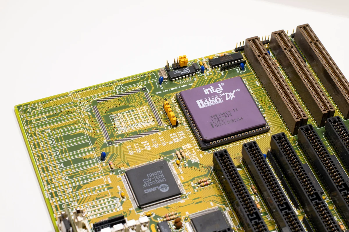
Visualizing Growth Techniques


Looking Ahead
As research progresses, the potential applications of controlled 2D semiconductor growth continue to expand. From more efficient solar cells to advanced computing systems, the future is bright for those who master this technology. However, challenges remain in scaling these techniques for mass production.
The road to mastering 2D semiconductor growth is filled with challenges, but the rewards are too great to ignore. As we push the boundaries of what’s possible, these materials will become the foundation of tomorrow’s technology. For developers, engineers, and researchers alike, the journey to control 2D growth is a path toward a future where chips are not only smaller and faster but also more efficient and powerful than ever before.